


Head Office
141-A, Electronic complex, Pardesipura,Indore - 452010 India
Phone: +91 73899 00887 , +91 98932 70303
Toll Free
+91 73899 00887
Working Hours
We are happy to meet you during our working hours. Please make an appointment.
- Monday-Saturday: 9:00 AM - 5:30 PM (IST)
- Sunday: Closed
Head Office
141-A, Electronic complex, Pardesipura,Indore - 452010 India
Phone: +91 73899 00887 , +91 98932 70303
Toll Free
+91 73899 00887
We are happy to meet you during our working hours. Please make an appointment.
- Monday-Saturday: 9:00 AM - 5:30 PM (IST)
- Sunday: Closed
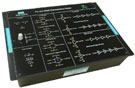
Experimentation with Characteristics of TTL and CMOS
Nvis 6551A
Product Description
Nvis 6551A Experimentation with Characteristics of TTL and CMOS is a compact product designed to explain the fundamentals of Transistor�Transistor Logic (i.e. TTL) and Complementary Metal Oxide Semiconductor (i.e. CMOS), like Voltage Transfer Characteristics, Noise Margin and Gate Delay. Inbuilt Function Generator and DC supply is provided for ease of operation.
The Voltage Transfer Characteristic of a logic gate is a graph between gate output voltage and gate input voltage. Noise margin is the voltage difference by which the signal exceeds the threshold voltage for Logic Low or Logic High. Gate delay is the span of time starting from the instant when the input to a logic gate becomes stable, to the time that the output of that logic gate becomes stable.
Nvis 6551A, Experimentation with Characteristics of TTL and CMOS is an ideal platform to enhance education, training, skills & development amongs our young minds.
Product Features
- In-built variable DC power supply
- In-built Function generator
- Illustration of both TTL and CMOS ICs
- Online product tutorial
Scope of Learning
- To study the voltage transfer characteristics, noise margin and gate propagation delay of TTL NAND gate
- To study the voltage transfer characteristics and gate propagation delay of TTL Schmitt trigger NAND gate
- To study the voltage transfer characteristics, noise margin and gate propagation delay of TTL NOT gate
- To study the voltage transfer characteristics and gate propagation delay of TTL Schmitt Trigger NOT gate
- To study the voltage transfer characteristics, noise margin and gate propagation delay of CMOS NAND gate
- To study the voltage transfer characteristics and gate propagation delay of CMOS Schmitt trigger NAND gate
- To study the voltage transfer characteristics, noise margin and gate propagation delay of CMOS NOT gate
- To study the voltage transfer characteristics and gate propagation delay of CMOS Schmitt Trigger NOT gate Scope
- Request Quote
- Technical Specification